
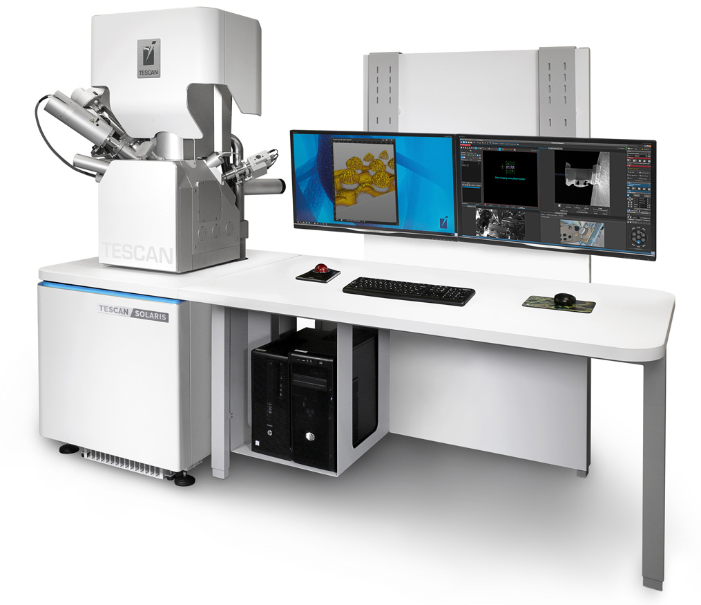

– Curtaining-free large-area cross-sectioning for physical failure analysis of advanced packaging technologies.
– Prepare large area FIB-cross-sections up to 1 mm wide.
– Obtain low noise, high-resolution image at low keVs in short acquisition time at FIB-SEM coincidence with the sample tilted.
– Live SEM-monitoring during FIB milling for precise end-pointing.
– Observe the most beam-sensitive materials using low keVs ultra-high resolution for surface sensitivity and high material contrast.
– Effective techniques and recipes for fast and artefact-free cross-sectioning of composite samples (OLED and TFT displays, MEMS devices, isolation dielectrics) at high currents
– Essence™ easy-to-use modular user interface
If you want more information about this equipment you must fill out the following form. Once completed, a direct download link will open.
Utilizamos cookies para melhorar a sua experiência no nosso site. Ao utilizar o nosso site, consente a utilização de cookies.
Gere abaixo as suas preferências de cookies:
Essential cookies enable basic functions and are necessary for the proper function of the website.
These cookies are needed for adding comments on this website.
Pode encontrar mais informações na nossa Cookie Policy e Política de privacidad.