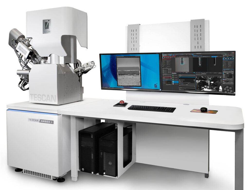
NEW iFIB+™ Xe plasma column
· High ion beam currents enable ultra-fast spray speeds.
· Unparalleled field of view: 1 mm at 30 keV.
· Variation of column opening through a piezoelectric system quickly and accurately
SEM UHR BrightBeam™ speaker technology
· Ultra-high-resolution fieldless SEM column for maximum versatility in sample analysis.
· Optimized beam detection system with increased detection efficiency and energy filtering capabilities
Benefits
· FIB blasting with gas-assisted Xe plasma with verified operating revenues
The combination of proprietary gas chemistry with Xe plasma FIB makes it possible to perform top-down planar etching on sub20 node technologies that are suitable for in situ nanoelectrical characterization. Our proven recipes guarantee excellent uniform planarity in windows that can be larger than 200 × 200 µm² and located anywhere on the chip.
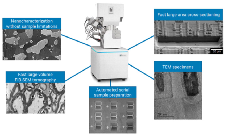
· Xe plasma FIB column with high ion beam currents and a large area field of view unmatched by other manufacturers that allows cross-sections over extremely large areas
The new iFIB+™ column enables a large 1mm field of view at 30 keV for easy and smooth sample navigation and in combination with high currents, extra large cross-sections in packages, MEMS and other large semiconductor technologies. Optoelectronic structures can be easily completed in short time frames.
This is a concrete solution to simplify complex failure analysis workflows for FEOL and BEOL processes.
· Make the most of the capabilities of electron and ion beams
The new OptiGIS™ is a fast, efficient and high-performance single gas injection system (GIS) essential in all your FIB applications. Up to 6 units can be installed for maximum versatility and multitasking configurations. Different proprietary gas chemicals are available for downstream planar IC removal.
Maximum accuracy and great FIB performance with ease
The new iFIB+™ column is equipped with an ultra-stable HV source and a precise piezo-driven beam aperture changer, enabling ultra-fast switching between FIB presets and high reproducibility. Additionally, a semi-automatic spot optimization wizard allows users to easily select the best beam spot that optimizes FIB milling conditions for the specific application.
· Adaptive spot shape optimization for better performance at high currents
The new TESCAN Essence™ software platform is a simplified multi-user user interface with a graphical design that allows quick and easy access to key functions. This easy-to-use interface can be customized to best suit the specific application, user skill level, and preferences. A wide variety of software modules, wizards, and recipes make FIB-SEM applications an easy, simple experience for new and experienced users, increasing productivity and helping to increase performance in the laboratory. The new TESCAN Essence™ also offers the Advanced DrawBeam™ vector-based sweep generator for fast and accurate FIB machining.
– Sample preparation without the use of Gallium preserves the physical properties of the samples unchanged.
· Maximum surface sensitivity and versatility in sample characterization
The BrightBeam™ SEM column provides ultra-high resolution fieldless imaging with excellent performance, especially at low beam energies. The electronic optics design, in combination with an optimized detection system, ensures excellent collection of electronic signals even at ultra-low electron beam energies without relying on beam deceleration for maximum sensitivity and surface versatility in sample characterization.
· Enhanced surface sensitivity and maximum contrast
The detection system with angle selection filtering and power filtering capabilities provides complete control of surface sensitivity and the option to scan with different contrasts.
· Reliability and the best conditions for microanalysis
The BrightBeam ™ SEM speaker comes with aperture optimization that results in improved resolution at high currents.