ELECTRONIC MICROSCOPY PRODUCTS
TESCAN SEM/STEM
Transmission scanning electron microscopy (STEM) is a combination of SEM and TEM: that is, a transmission image is obtained using a scanning method. A TEM can be modified into a STEM by adding a system that sweeps a focused beam through the sample to form the image. A very basic STEM can also be achieved by installing a transmission detector in an SEM.
Like TEM, STEM requires very thin samples and mainly analyzes the beam electrons transmitted by the sample. One of its main advantages over TEM is that it allows the use of other signals that cannot be spatially correlated in TEM.
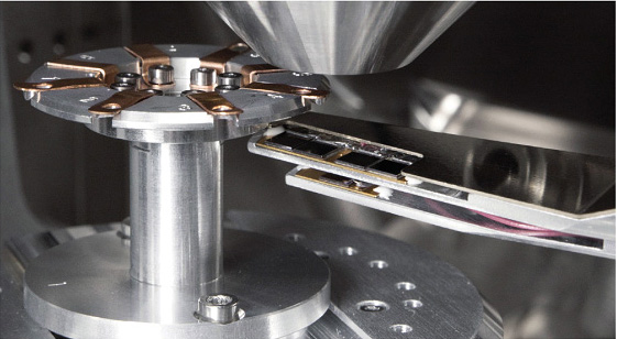
Detetor HADF R_STEM e porta-amostras múltiplas STEM.
In this case we are talking about the possibility of having a STEM image in a SEM. It would be the simplest possible form of STEM, but it can be very useful for us to complete the rest of the SEM images as a transmission image
These transmitting detectors will be very good for us to monitor and check the state of the lamellas that we prepared with a FIB without having to interrupt the process to observe them in a TEM.
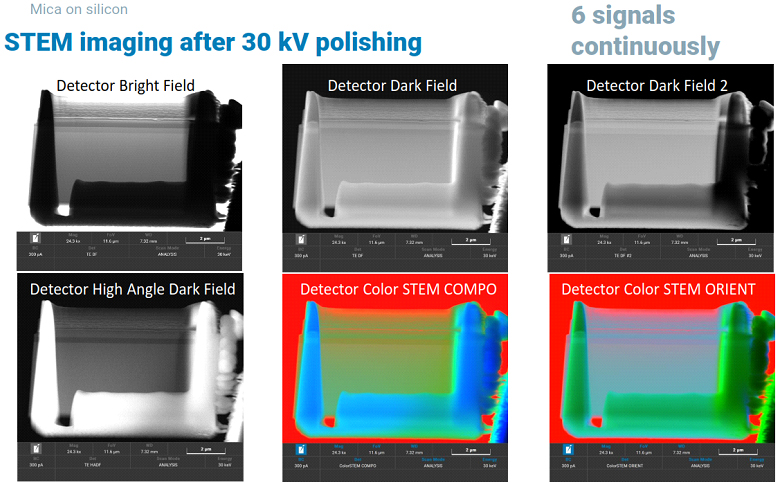
In the SEM / STEM we work at low acceleration voltages but we can achieve subnanometer resolutions (0.6 nm), which makes it a very efficient alternative from an economic point of view to a TEM / STEM.
Features:
• Observation of multiple samples without breaking the chamber vacuum.
• Simultaneous acquisition of brightfield (BF), darkfield (DF), and high-angle darkfield (HADF) signals that provide valuable information such as Bragg diffraction orientation contrast and material contrast.
• Increase and decrease the height of the sample in relation to the detector to obtain the best imaging conditions.
• Tilt the sample independently of the detector.
• Improved sample holder geometry for EDX analysis.
