
ELECTRONIC MICROSCOPY PRODUCTS
TEM microscopes
Transmission electron microscopy (TEM) is a technique for high-resolution imaging of thin samples.
A beam of high-energy electrons passes through the sample and is then focused to form an image. When samples are less than one micron thick, we can use a transmission electron microscope or TEM for imaging, but if we want to do electron diffraction, the thickness must be less than 100 nm.
The resolution of TEM is greater than that of the scanning electron microscope and is typically on the order of 0.2 nm.
The electron wavelength is related to the accelerating voltage, so excluding the rest of the parameters (e.g. e-interaction volume), the resolution of an electron microscope will be higher at a higher accelerating voltage. SEMs reach 30 kV, while we have TEMs of 120 kV, 200 kV and 400 kV. Higher accelerating voltages provide greater resolution but less contrast. TEMs allow us to reach the highest resolutions and see the atomic configurations of nanostructures.
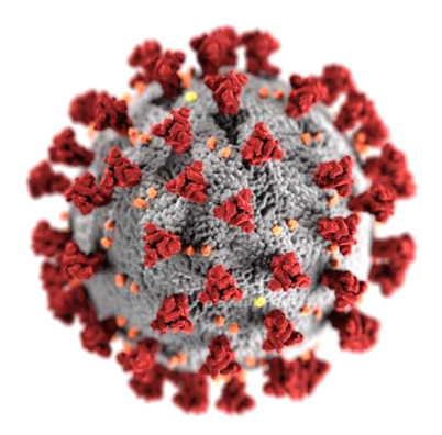
TEM TOMOGRAPHY of a COVID-19 electron tomography can be obtained by recording images in a series of different projections of the sample and then mathematically recombining these images to form a three-dimensional representation of the sample.
Bright field: Thicker regions of the sample or regions with higher atomic numbers will appear dark, while non-sample regions in the beam path will appear bright: Morphology.
Diffraction contrast: Since electrons have wave properties, they can be diffracted by crystalline samples. The resulting diffraction patterns provide information about the crystal structure of the sample. The contrast is formed by the incident electrons spread elastically across the nuclei. The image obtained provides information about the orientation, arrangement of atoms and the phases present in the area examined.
Crystallography: Diffraction contrast in TEM gives us information about:
1) The phases and types of crystalline structure.
2) Crystal symmetry and space group.
3) Orientation relationships between phases.
4) Determine growth directions, interface coherence.
5) Identification of defects, i.e. twinning, SF, dislocations,
6) Ordering behavior of crystalline structures and site occupation preferences…
Sign of loss of electronic energy: the contrast is formed by the inelastic scattering of incident electrons. They provide composition and state information about atomic bonds. REDOX chemical state.

TESCAN SEM/STEM solutions


TESCAN TENSOR
The first integrated, precession-assisted and analytical near-UHV 4D-STEM.